
LNK304PN 5v Buck converter output problem
Hi
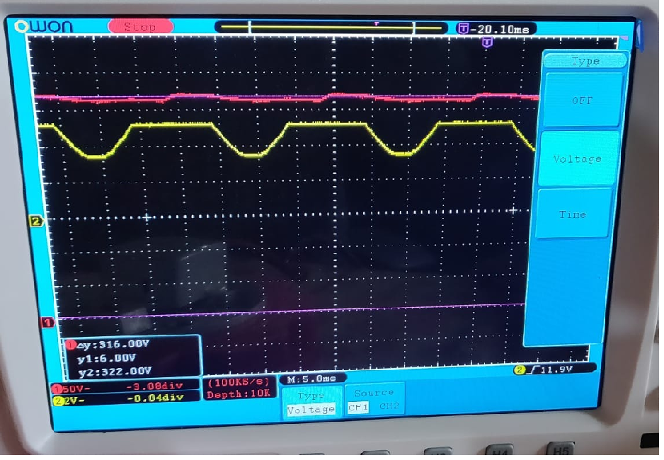
I have configured LNK304PN IC to give 5V Output as shown in the attached schematic file. I have attached image of 5V which i am getting from oscilloscope.
Please help me to get pure 5V DC output.
Below are specification of components
Supply used 220V AC 50Hz
After rectification Drain pin is getting 310V DC
Rfb=10k
Rbias=5.1k
Cbp=0.1uf
Cfb=10uf
L1=1.2mH and also L1 = 680uH
Cout i tried different values = 1uf, 10uf , 470uf
at the output their is voltage drop of 1.2 to 1.8V after every 10ms. I have checked the Drain input pin and i m getting 310V DC without voltage dips.
Files
| Attachment | Size |
|---|---|
| Schematic.png | 29.47 KB |
| Red channel is Drain input_Yellow channel is 5V output | 759.46 KB |
Comments
For load i tried with different combinations
13K ohm load resistor for which current will be 380mA.
27K ohm load resistor for which current will be 180mA
47k ohm load resistpr for which current will be 106mA
their is variation in voltage with respect to change in load resistors but the DC output remains same with voltage dropping to 1.8V in every alternating cycle of 10ms as shown in the attached image.
Input voltage is 220V to 230V AC with 50Hz before the bridge rectifier.
after bridge rectifier i am getting (peak) 310V DC when capture from the scope.
I have attached the image for the same above.
| Attachment | Size |
|---|---|
| first_channel_Drain_input_2nd_channel_Output_voltage.png | 759.46 KB |
Hi Thejest
There is an online design tool that can help in the selection of parts.
Please refer to below link for the Design Tool - PIExpert Online
https://piexpertonline.power.com/
I have use PIExpert online to create a Design for
85Vac - 265Vac Input
5V output
170mA output Current (Max Io for LNK304 based on the datasheet)
Bridge Diode = Full Bridge
Please see attach file.
The PIExpert recommends also parts value of the Buck topology.
Please use the recommended feedback resistor based on the PIExpert.
As per datasheet Rbias should be 2kohms. This ensure good noise immunity
The datasheet also contains information on the design recommendation of LNL TN series.
Application notes AN-37 is a design guide for LNK TN ICs.
Are you using Full bridge rectifier or half bridge rectifier in the input side?
The schematics that you have forwarded contains only one diode on the input side.
Thanks
| Attachment | Size |
|---|---|
| LinkSwitch-TN_Buck_Design2.pdf | 460.4 KB |
Hi Chloe,
I tried with the above specified resistor combination, even then the output is same. half sine wave in the dc output every 10ms.
I am using GBU810 Bridge rectifier. Do you think Bridge rectifier is causing the issue??
But when i see the input voltage to the Drain of the LNK304 IC, it seems ok at 316V DC. as shown in the previously attached image.
Datasheet of GBU810 says -Non-Repetitive Peak Forward Surge Current 8.3ms
single half sine-wave superimposed on rated load IFSM- 200Amps., Do you think this is causing the issues. please verify me once.
I will try with other Bridge rectifier and i will update results as well.
Regards,
Thejesh
LNK304P is not recommended for new designs mentioned in datasheet of LNK304P.
Hi Imran Ahmed,
please suggest alternate IC for LNK304P, for generating 5V 150ma or 200ma output.
it will be good if footprint remains same.
Regards,
Thejesh
Hi Thejesh
POWI is still supporting LNK304P and this is an active product.
But, we are proposing to use LNK TN2 series instead of LNK TN.
Now, concern will be that LNK TN2 and LNK TN have different pin outs.
Please draw you complete circuit that includes the half bridge or full bridge rectifier and input AC source.
Includes the location of the prove positive and probe negative
I think the dipping of the 5V coincides with the input AC.
Thanks
Regards
Patrick
Hello Patrick,
I have attached the complete circuit. please look into it
I also tried with replacing the ic, the output is same with negative voltage
it is same across bypass capacitor as well where we get 5.8V
Regards,
Thejesh
| Attachment | Size |
|---|---|
| Schematic.pdf | 59.19 KB |
Hi Thejesh,
The circuit have D2 (bridge rectifier). D9 can be remove.
Or do you have any reason in adding D9
What is the purpose of T2?
Thanks
Regards
PI-Chloe
Hi Chloe,
T2 is line transformer (1:1) for giving isolation for the secondary circuit.
Yes D2 is Bridge rectifier, D9 was used to block negative voltages/ leakage current.
I will try removing D9 and update u the results.
Regards,
Thejesh
Hi Thejesh
Can you also send me screen shot of the PCB lay out.
Thanks
Regards
Patrick
Hi Thejesh
Thanks for using Power Integration products.
May I know the maximum load current of the 5V output?
What is the input voltage range of your design?
Thanks
Regards